Photo AI
A silicon-based 5.1 V Zener diode requires a minimum operating current I of 5.0 mA to maintain its Zener voltage Vz - AQA - A-Level Physics - Question 4 - 2019 - Paper 8
Question 4
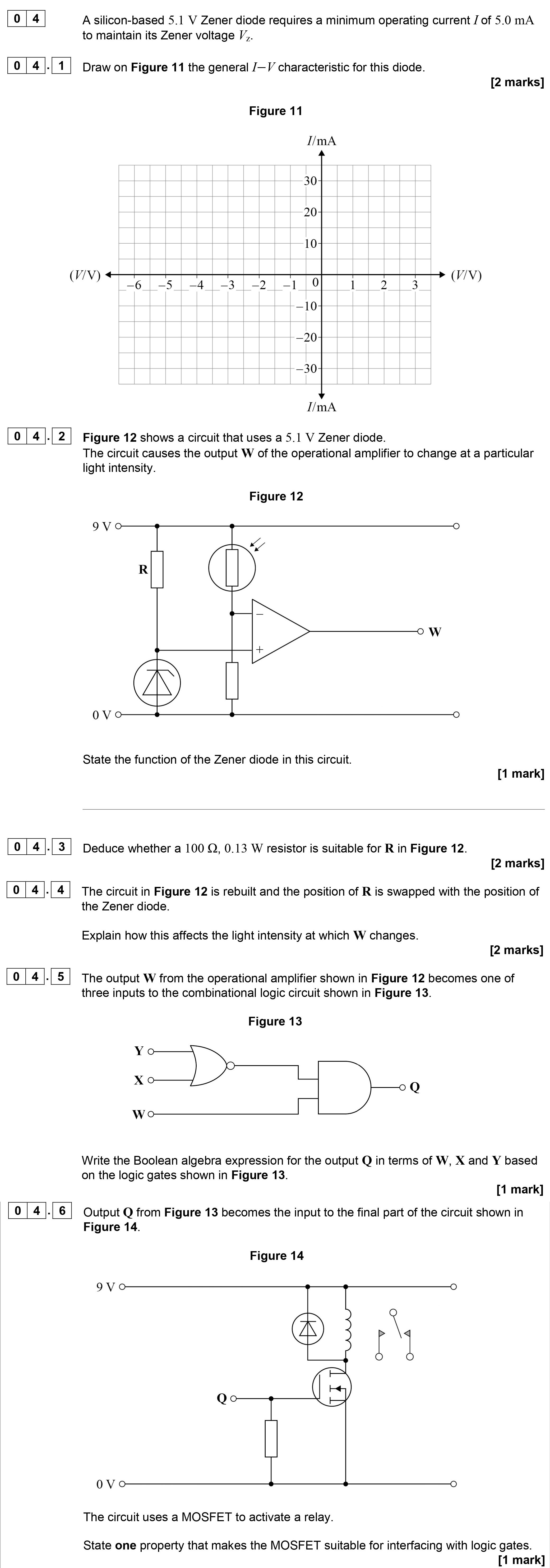
A silicon-based 5.1 V Zener diode requires a minimum operating current I of 5.0 mA to maintain its Zener voltage Vz. Draw on Figure 11 the general I-V characteristi... show full transcript
Worked Solution & Example Answer:A silicon-based 5.1 V Zener diode requires a minimum operating current I of 5.0 mA to maintain its Zener voltage Vz - AQA - A-Level Physics - Question 4 - 2019 - Paper 8
Step 1
Draw on Figure 11 the general I-V characteristic for this diode.

Answer
The I-V characteristic curve for a Zener diode typically shows a flat region where the diode maintains a constant voltage (5.1 V) despite increases in current. The curve should rise steeply in the forward-biased region and remain relatively flat in the reverse-biased region until the Zener breakdown voltage is reached.
Step 2
State the function of the Zener diode in this circuit.
Answer
The Zener diode provides a reference voltage or stabilizes the output voltage of the operational amplifier by clamping to its Zener voltage of 5.1 V. It ensures that the voltage at the non-inverting input does not exceed this value.
Step 3
Deduce whether a 100 Ω, 0.13 W resistor is suitable for R in Figure 12.
Answer
To determine the suitability of the 100 Ω resistor, calculate the current through it using Ohm's law. The power dissipated by the resistor can be calculated using the formula:
For I = 5 mA:
Since 0.025 W is less than 0.13 W, the resistor is suitable.
Step 4
Explain how this affects the light intensity at which W changes.
Answer
Swapping the positions of the resistor R and the Zener diode will change the voltage at the non-inverting input of the operational amplifier. It will result in a different reference voltage being applied, leading to a different threshold at which the light intensity (represented by W) varies. As a result, the light intensity may be lower than before, as the Zener diode might now be in a position that doesn't maintain the same voltage across the light sensor.
Step 5
Step 6
State one property that makes the MOSFET suitable for interfacing with logic gates.
Answer
A MOSFET has a large input impedance, which ensures that it does not significantly load the output of the logic gate it is interfacing with. This high input impedance allows for minimal current draw from the previous stage, maintaining signal integrity.