Photo AI
A p-n junction (diode) is formed by doping adjacent layers of a semiconductor - Leaving Cert Physics - Question c - 2009
Question c
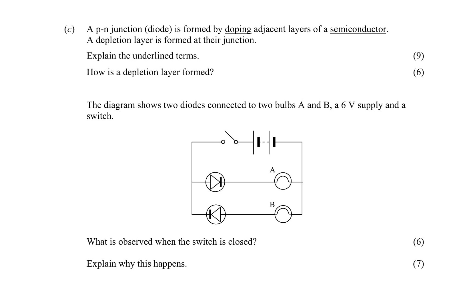
A p-n junction (diode) is formed by doping adjacent layers of a semiconductor. A depletion layer is formed at their junction. Explain the underlined terms. How is ... show full transcript
Worked Solution & Example Answer:A p-n junction (diode) is formed by doping adjacent layers of a semiconductor - Leaving Cert Physics - Question c - 2009
Step 1
Explain the underlined terms.

Answer
-
Doping: Doping is the process of adding impurities to a semiconductor to change its electrical properties. By adding specific elements, the conductivity of the semiconductor can be increased, transforming it into either a p-type or n-type material. In p-type doping, elements such as boron are added, creating 'holes' (positive charge carriers), whereas n-type doping involves adding elements like phosphorus, providing extra electrons (negative charge carriers).
-
Semiconductor: A semiconductor is a material that has a conductivity level between that of a conductor (like metals) and an insulator (like glass). Semiconductors are essential in forming diodes and transistors, and their resistivity can be manipulated through doping.
Step 2
How is a depletion layer formed?
Answer
A depletion layer is formed at the junction of p-type and n-type semiconductors. When these two types of materials come into contact, holes from the p-type region diffuse into the n-type region and recombine with electrons there. Consequently, an area devoid of charge carriers develops near the junction, known as the depletion region. This region presents an electric field that prevents further movement of carriers, thus stabilizing the diode.
Step 3
Step 4
Explain why this happens.
Answer
Bulb A lights up because the diode connected to it is in the forward-biased condition, allowing current to flow. In contrast, bulb B does not light up because its diode is in reverse-biased condition, preventing any current to pass through, thus illuminating only bulb A.