Logic Gates (AQA A-Level Computer Science): Revision Notes
Logic Gates
Introduction
Logic gates are fundamental electronic components found in computer processors, memory chips, and registers. They work by evaluating Boolean expressions to produce digital outputs. Understanding logic gates is essential because there is a direct one-to-one relationship between Boolean expressions and the gates that implement them in hardware.
In electronic circuits, logic gates process electrical signals represented as voltages. A high voltage represents a binary 1 (true), whilst a low voltage represents a binary 0 (false). These gates form the building blocks of all digital circuits, from simple calculators to complex computer processors.
Logic gates are represented using standard symbols in circuit diagrams, and each gate has a corresponding truth table that shows all possible input combinations and their resulting outputs. Each gate also has a Boolean operator that expresses its logical function mathematically.
The six basic logic gates
There are six fundamental logic gates that you need to understand. Each gate performs a specific logical operation on its inputs to produce a single output.
Here is a summary of the six gates with their operators:
| Gate | Operator | Description |
|---|---|---|
| AND | A·B | Output is true only when both inputs are true |
| OR | A+B | Output is true when at least one input is true |
| NOT | Ā | Output is the inverse of the input |
| NAND | A·B̄ | Output is true when any input is false |
| NOR | Ā+B̄ | Output is true only when both inputs are false |
| XOR | A⊕B | Output is true when inputs are different |
Memorization Tip: Remember NAND and NOR as "NOT AND" and "NOT OR" - they produce the opposite outputs of their base gates (AND and OR).
AND gate
The AND gate produces a true output (1) only when both of its inputs are true. Think of it like a security system that requires two keys to open - both conditions must be met for the output to be true.
The Boolean expression for an AND gate is written as or , which means "A AND B".
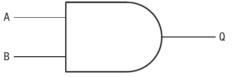
Here is the truth table for a 2-input AND gate:
| A | B | Q |
|---|---|---|
| 0 | 0 | 0 |
| 0 | 1 | 0 |
| 1 | 0 | 0 |
| 1 | 1 | 1 |
Notice that the output Q is only 1 in the final row, where both A and B are 1. In all other cases, the output is 0.
OR gate
The OR gate produces a true output (1) when either one or both of its inputs are true. Only when both inputs are false does the output become false. This is similar to a light that can be switched on from two different locations - either switch (or both) can turn it on.
The Boolean expression for an OR gate is , which means "A OR B".
The truth table for a 2-input OR gate is:
| A | B | Q |
|---|---|---|
| 0 | 0 | 0 |
| 0 | 1 | 1 |
| 1 | 0 | 1 |
| 1 | 1 | 1 |
The output is 1 whenever at least one input is 1. The output is only 0 when both inputs are 0.
NOT gate
The NOT gate is unique because it has only one input. It inverts whatever value is input - turning 1 into 0 and 0 into 1. This is also called an inverter.
The Boolean expression is or NOT A, which means "NOT A" or "the inverse of A".
The truth table for a NOT gate is:
| A | Q |
|---|---|
| 0 | 1 |
| 1 | 0 |
The NOT gate is often represented with a small circle (bubble) at the output of the gate symbol, indicating inversion. You'll see this bubble used in NAND and NOR gates as well.
NAND gate
The NAND gate is essentially an AND gate followed by a NOT gate. Its name means "NOT AND". The output is true (1) when any of the inputs are false - it's the opposite of the AND gate.
The Boolean expression is , which means "NOT (A AND B)".
The truth table for a 2-input NAND gate is:
| A | B | Q |
|---|---|---|
| 0 | 0 | 1 |
| 0 | 1 | 1 |
| 1 | 0 | 1 |
| 1 | 1 | 0 |
Notice this is the exact opposite of the AND gate - wherever the AND gate produces 0, the NAND gate produces 1, and vice versa. The NAND gate symbol looks like an AND gate with a small circle (bubble) at the output, indicating the inversion.
NOR gate
The NOR gate is an OR gate followed by a NOT gate. Its name means "NOT OR". The output is true (1) only when both inputs are false - it's the opposite of the OR gate.
The Boolean expression is , which means "NOT (A OR B)".
The truth table for a 2-input NOR gate is:
| A | B | Q |
|---|---|---|
| 0 | 0 | 1 |
| 0 | 1 | 0 |
| 1 | 0 | 0 |
| 1 | 1 | 0 |
This is the inverse of the OR gate truth table. The NOR gate symbol looks like an OR gate with a small circle at the output.
XOR gate (exclusive OR)
The XOR gate stands for "exclusive OR". It produces a true output (1) when either input is true, but not when both inputs are true. In other words, the output is true when the inputs are different from each other.
The Boolean expression is , which means "A XOR B".
The truth table for a 2-input XOR gate is:
| A | B | Q |
|---|---|---|
| 0 | 0 | 0 |
| 0 | 1 | 1 |
| 1 | 0 | 1 |
| 1 | 1 | 0 |
The XOR gate is particularly useful in arithmetic circuits for detecting when two bits are different, which is essential in addition operations. You'll see XOR gates used extensively in adder circuits.
Combining logic gates
Logic circuits are created by connecting multiple logic gates together in sequence. These circuits can become very complex, with thousands of gates working together in modern processors. The output from one gate becomes the input to the next gate, creating a chain of logical operations.
When you combine gates, you build up more complex Boolean expressions. Each intermediate connection represents a partial result that feeds into the next stage of processing.
Worked Example: Alarm System Logic Circuit
Let's look at an alarm system with two sensors (A and B) and a manual override switch (C):
- When A or B equals 1, a sensor has detected an intruder
- When C equals 1, the override button has been pressed to turn off the alarm
- The alarm should sound only if a sensor is triggered AND the override hasn't been pressed
This can be expressed as: , which means "(A OR B) AND (NOT C)".
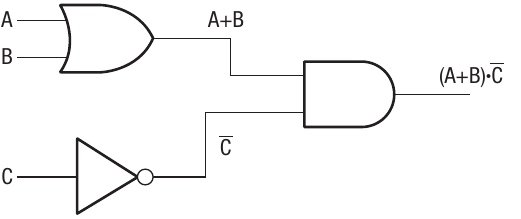
Step-by-step circuit operation:
Step 1: Inputs A and B pass through an OR gate, producing the result
Step 2: Input C passes through a NOT gate, producing (NOT C)
Step 3: These two results then pass through an AND gate to create the final output
The truth table for this circuit shows all possible input combinations:
| A | B | C | Q |
|---|---|---|---|
| 0 | 0 | 0 | 0 |
| 0 | 0 | 1 | 0 |
| 0 | 1 | 0 | 1 |
| 0 | 1 | 1 | 0 |
| 1 | 0 | 0 | 1 |
| 1 | 0 | 1 | 0 |
| 1 | 1 | 0 | 1 |
| 1 | 1 | 1 | 0 |
Notice that Q is only 1 when at least one sensor is triggered (A or B is 1) and the override is not pressed (C is 0).
Building Boolean expressions from logic circuits
Just as you can create a logic circuit from a Boolean expression, you can also work backwards to create a Boolean expression from a circuit diagram. You simply follow the signal path through each gate, writing down the operation performed at each stage.
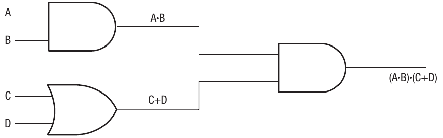
For more complex circuits, you trace through each gate systematically:
- Identify the inputs entering the first layer of gates
- Write the Boolean expression for each gate's output
- Use these intermediate results as inputs to the next layer of gates
- Continue until you reach the final output
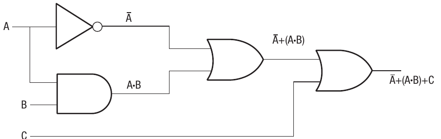
As circuits become more complex, the Boolean expressions grow longer and more intricate. This demonstrates why modular design is important in digital electronics - breaking complex operations into smaller, manageable components.
Full and half adders
Adders are special logic circuits designed to perform binary addition. They are fundamental components of the Arithmetic Logic Unit (ALU) in a processor, which handles all mathematical and logical operations.
Half adder
A half adder is a circuit that adds two single bits together (A and B). It produces two outputs:
- S (Sum): the sum of A and B
- C (Carry): the carry bit generated when both inputs are 1
Worked Example: Binary Addition with Half Adder
When you add two bits in binary:
- (sum = 0, carry = 0)
- (sum = 1, carry = 0)
- (sum = 1, carry = 0)
- in binary (sum = 0, carry = 1)
The last case shows why we need the carry bit - when adding , we get in binary (which is in decimal), so the sum is and we carry to the next column.
The half adder uses an XOR gate to calculate the sum (S) because the XOR gate outputs 1 when the inputs are different. It uses an AND gate to calculate the carry (C) because a carry is only generated when both inputs are 1.
The truth table for a half adder is:
| A | B | C | S |
|---|---|---|---|
| 0 | 0 | 0 | 0 |
| 1 | 0 | 0 | 1 |
| 0 | 1 | 0 | 1 |
| 1 | 1 | 1 | 0 |
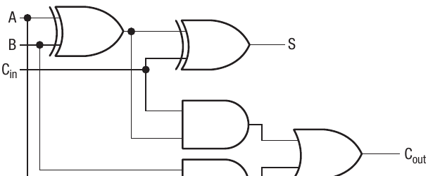
Full adder
A half adder can only add two bits, but what if you need to add multiple bits or include a carry from a previous addition? This is where the full adder comes in.
A full adder adds three inputs:
- A: first bit
- B: second bit
- Cin: carry input from a previous addition
It produces two outputs:
- S (Sum): the sum result
- Cout: the carry output for the next addition
Full adders can be chained together to add multi-bit binary numbers. The carry output (Cout) from one full adder becomes the carry input (Cin) to the next full adder in the chain. This is why Cout from the first addition becomes Cin for the second addition, and so on.
The truth table for a full adder shows all eight possible input combinations:
| A | B | Cin | Cout | S |
|---|---|---|---|---|
| 0 | 0 | 0 | 0 | 0 |
| 1 | 0 | 0 | 0 | 1 |
| 0 | 1 | 0 | 0 | 1 |
| 1 | 1 | 0 | 1 | 0 |
| 0 | 0 | 1 | 0 | 1 |
| 1 | 0 | 1 | 1 | 0 |
| 0 | 1 | 1 | 1 | 0 |
| 1 | 1 | 1 | 1 | 1 |
The full adder circuit works as follows:
- First XOR gate compares A and B to see if they're different
- Second XOR gate combines that result with Cin to produce the sum
- AND gates and OR gate work together to determine if a carry should be generated
- A carry is produced when either both original inputs are 1, or when the result of A and B produces a 1 that combines with Cin
Edge-triggered D-type flip-flop (A-level only)
Whilst logic gates show how binary values can be manipulated, they don't store data. Each time new inputs arrive, the previous results are lost. In real computer systems, we need some way to remember values temporarily - this is where flip-flops come in.
A flip-flop is a memory unit that can store a single bit of information. The edge-triggered D-type flip-flop is a specific type that changes its stored value only when triggered by the system clock.
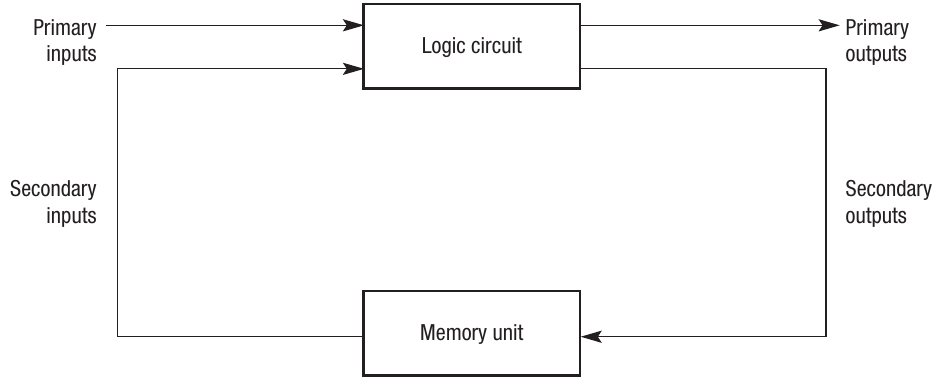
The system diagram shows two types of inputs:
- Primary inputs: direct inputs to the logic circuit
- Secondary inputs: inputs that come from the memory unit (feedback from previous operations)
Similarly, there are two types of outputs:
- Primary outputs: the main results of the computation
- Secondary outputs: values sent back to the memory unit for storage
This feedback mechanism allows the system to maintain state - remembering previous results and using them in future calculations. This is essential for sequential circuits that depend on history, not just current inputs.
Clock signals
The clock is a device that generates regular pulses to synchronise all components in a computer. These pulses ensure that data moves through the system in an orderly, predictable manner.
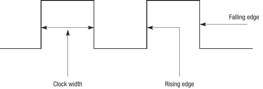
A clock signal has several important characteristics:
Clock period: the time for one complete cycle (one pulse) of the clock
Clock width: the duration of the high portion of the pulse
Rising edge: the transition from low (0) to high (1) voltage - this is when the signal goes up
Falling edge: the transition from high (1) to low (0) voltage - this is when the signal goes down
How the D-type flip-flop works
An edge-triggered D-type flip-flop changes its state only on one edge of the clock pulse (usually the rising edge). This means:
- Data present at the input when the clock pulse arrives gets stored in the flip-flop
- This stored data remains at the output until the next clock pulse arrives
- Any changes to the input between clock pulses are ignored
Why synchronization matters:
This behaviour is crucial for synchronising operations. Without it, data could change at unpredictable times, causing errors. With edge-triggered flip-flops, all changes happen at precisely defined moments determined by the clock.
For example, if you're adding numbers in the ALU, the flip-flops ensure that:
- The inputs remain stable whilst the addition is being calculated
- The result is stored at a predictable time
- This result can then be used as input for the next operation on the next clock cycle
This synchronisation is fundamental to how modern processors execute billions of instructions per second in an orderly, controlled manner.
Remember!
Key Points to Remember:
-
Logic gates are the building blocks of all digital circuits - they implement Boolean expressions in hardware using high and low voltages to represent 1s and 0s.
-
There are six basic gates to memorise: AND (both inputs true), OR (at least one input true), NOT (inverts input), NAND (not both true), NOR (neither true), and XOR (inputs different).
-
Gates combine to create complex circuits where the output of one gate feeds into the input of another, building up complex Boolean expressions step by step.
-
Adders perform binary addition - half adders add two bits producing a sum and carry, whilst full adders add three bits (including carry in) and are chained together for multi-bit addition in the ALU.
-
Flip-flops provide memory - edge-triggered D-type flip-flops store single bits and only change state on clock edges, providing the synchronisation needed for sequential circuits to maintain state and process data in an orderly manner.