Properties of Semiconductors (Leaving Cert Engineering): Revision Notes
Properties of Semiconductors
What are semiconductors?
Semiconductors are materials that have electrical properties positioned between those of conductors and insulators. They represent a unique class of materials that can conduct electricity, but not as easily as metals, and much better than insulators.
The name "semiconductor" literally means "half conductor" - indicating their intermediate electrical behaviour. This naming perfectly captures their position between full conductors (like metals) and non-conductors (insulators).
These materials have become fundamental to modern technology, forming the basis of all electronic devices including computers, smartphones, and solar panels.
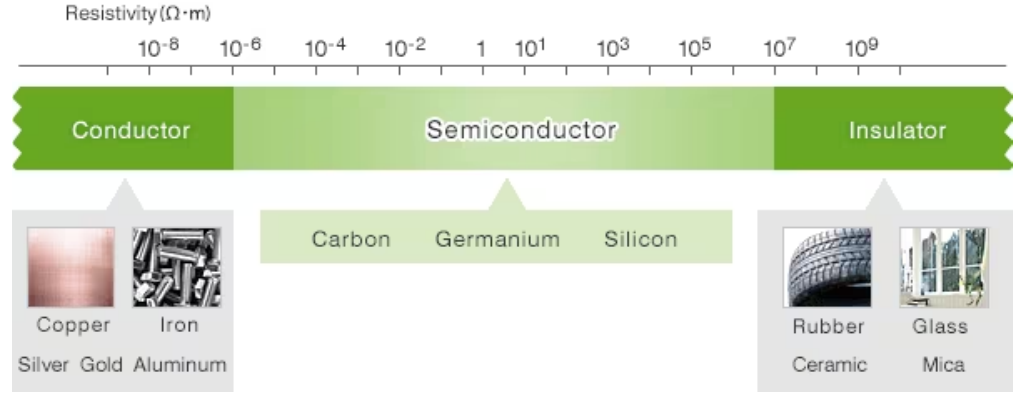
The resistivity chart above shows how semiconductors fit between conductors and insulators on the electrical resistivity spectrum. Resistivity is measured in ohm-meters (Ω·m) and indicates how strongly a material opposes electrical current flow.
Key semiconductor materials include:
- Silicon - the most widely used semiconductor
- Germanium - historically important, still used in some applications
- Carbon - in specific forms can act as a semiconductor
Energy band theory
To understand how semiconductors work, we need to examine their atomic structure and energy band theory. This theory explains why different materials conduct electricity differently.
Atomic structure and energy levels
Atoms consist of a nucleus surrounded by electrons in specific energy levels. When many atoms join together to form a solid material, these individual energy levels combine to create energy bands.
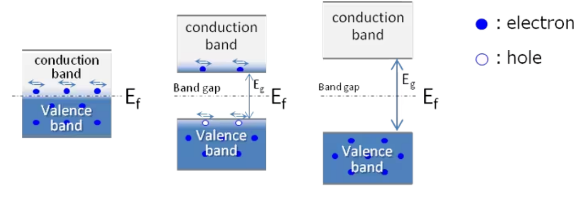
The energy band diagram shows three important regions:
- Valence band - where electrons are normally found at low temperatures
- Conduction band - where electrons can move freely and conduct electricity
- Band gap (Eg) - the energy difference between valence and conduction bands
Comparing different materials
Understanding how different materials behave electrically requires examining their energy band structures:
Metals (conductors): In metals, the valence band and conduction band overlap or are very close together. This means electrons can move freely between bands, creating excellent electrical conductivity. The Fermi energy (Ef) lies within the conduction band, ensuring there are always free electrons available for current flow.
Insulators: Insulators have a very large band gap between the valence and conduction bands. This massive energy barrier prevents electrons from jumping to the conduction band under normal conditions, resulting in extremely poor electrical conductivity.
Semiconductors: Semiconductors have a moderate band gap - smaller than insulators but larger than metals. At room temperature, some electrons can gain enough thermal energy to jump across this gap and conduct electricity, but not as many as in metals.
The key difference between these materials lies in their band gap size:
- Metals: Band gap ≈ 0 eV (overlapping bands)
- Semiconductors: Band gap ≈ 0.1-4 eV
- Insulators: Band gap > 4 eV
This determines their electrical conductivity at room temperature.
Temperature effects on conductivity
The electrical behaviour of semiconductors changes dramatically with temperature, which is one of their most distinctive characteristics:
At low temperatures:
- Very few electrons have enough energy to cross the band gap
- Semiconductors behave almost like insulators
- Electrical conductivity is very low
At room temperature:
- Thermal energy allows some electrons to jump to the conduction band
- Limited electrical conductivity develops
- This is why semiconductors are called "half conductors"
At higher temperatures:
- More electrons gain sufficient energy to cross the band gap
- Electrical conductivity increases significantly
Key Temperature Effects:
- Lower temperature → Lower conductivity (more insulator-like)
- Higher temperature → Higher conductivity (more conductor-like)
- This temperature-dependent behaviour makes semiconductors useful in temperature sensors and other electronic applications
Doping - creating n-type and p-type semiconductors
Pure semiconductors have limited practical applications. To make them useful in electronic devices, we add tiny amounts of impurities through a process called doping.
The doping process transforms pure semiconductors into materials with controlled electrical properties by strategically adding specific impurities.
n-type semiconductors
n-type semiconductors are created by adding donor impurities to pure semiconductor material:
Creating n-type Silicon:
Step 1: Start with pure silicon (Si) - each atom has 4 outer electrons
Step 2: Add phosphorus (P) atoms - each has 5 outer electrons
Step 3: The extra electron from phosphorus becomes available for conduction
Step 4: Result: n-type semiconductor with mobile electrons
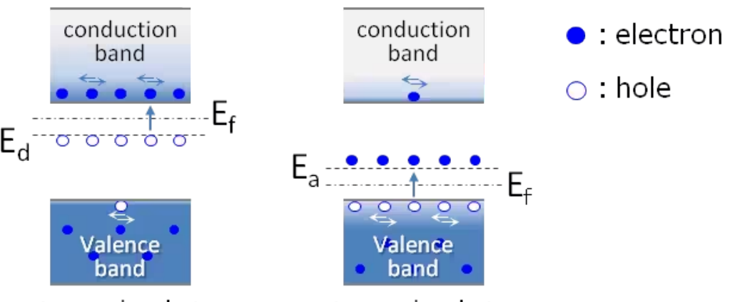
- Donors are typically pentavalent elements like phosphorus (P) or arsenic (As)
- These atoms have five outer electrons compared to silicon's four
- The extra electron becomes available for conduction
- Donor energy level (Ed) is close to the conduction band
- Electrons easily jump from donor level to conduction band
- "n-type" stands for "negative" due to the extra negative electrons
p-type semiconductors
p-type semiconductors are created by adding acceptor impurities:
Creating p-type Silicon:
Step 1: Start with pure silicon (Si) - each atom has 4 outer electrons Step 2: Add boron (B) atoms - each has only 3 outer electrons Step 3: This creates "holes" (missing electrons) in the crystal structure Step 4: Result: p-type semiconductor with mobile holes
- Acceptors are typically trivalent elements like boron (B)
- These atoms have only three outer electrons
- This creates "holes" (missing electrons) in the valence band
- Acceptor energy level (Ea) is close to the valence band
- Electrons from the valence band can fill these acceptor levels
- This leaves behind holes that can move and conduct electricity
- "p-type" stands for "positive" due to the positive holes
High purity requirements
Critical Manufacturing Requirement:
Semiconductor manufacturing requires extremely pure starting materials. For example, silicon used in integrated circuits must be 99.9999999% pure. Even tiny amounts of the wrong impurities can dramatically affect electrical properties.
This level of purity is equivalent to one impurity atom per billion silicon atoms!
Practical applications
The controllable electrical properties of semiconductors make them essential for modern electronics:
- Transistors - switching and amplifying electrical signals
- Diodes - allowing current flow in one direction only
- Solar cells - converting light energy to electrical energy
- Light-emitting diodes (LEDs) - converting electrical energy to light
- Integrated circuits - complex electronic systems on single chips
The global semiconductor industry produces trillions of electronic components annually, making semiconductors one of the most important material technologies in human history.
Key Points to Remember:
- Semiconductors have electrical properties between conductors and insulators
- Energy band theory explains electrical behaviour through valence bands, conduction bands, and band gaps
- Temperature affects semiconductor conductivity - higher temperature means better conduction
- n-type semiconductors have extra electrons from donor impurities
- p-type semiconductors have holes from acceptor impurities
- Doping allows precise control of electrical properties
- Ultra-high purity is essential for semiconductor manufacturing