Production of Semiconductors (Leaving Cert Engineering): Revision Notes
Production of Semiconductors
Introduction to semiconductor manufacturing
Semiconductor production involves creating complex electronic components that contain billions of tiny parts including transistors, diodes, resistors, and capacitors. These components must work together precisely to perform logic operations and store data in devices we use every day.
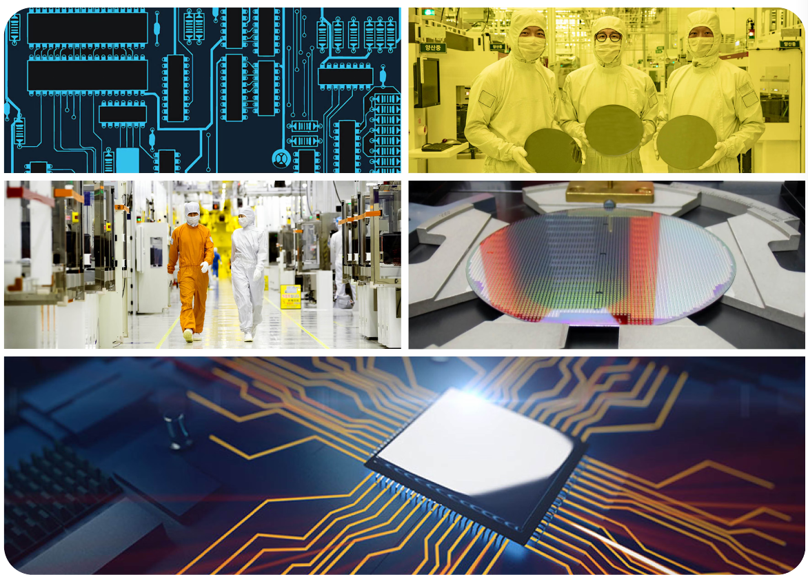
The manufacturing process transforms raw silicon into sophisticated integrated circuits (ICs) through eight main steps. Each step requires extremely precise control and takes place in ultra-clean environments to prevent contamination.
Modern semiconductor chips may appear small, but they pack enormous complexity into their fingernail-sized structure. A single chip can contain over 50 billion transistors, each smaller than a virus!
Understanding how these circuits are made helps explain why semiconductor technology is so advanced and expensive to produce.
Step 1: Building and protecting the silicon wafer
Creating the silicon foundation
The production process begins with preparing the silicon wafer, which serves as the foundation for building circuits. Think of the wafer as the chip's canvas - a thin, flat disc that provides the base for all subsequent manufacturing steps.
Silicon extraction and purification:
- Silicon starts as ordinary sand
- The sand undergoes purification processes
- Pure silicon gets formed into a large cylindrical block called an ingot
Wafer preparation:
- The cone-shaped ends of the ingot are removed while still hot
- The remaining cylinder gets sliced into wafers of uniform thickness
- Larger wafers increase productivity - the current industry standard uses 12-inch diameter wafers
Surface preparation and protection
Before circuits can be built, the wafer surface requires careful preparation:
Polishing process:
- Abrasive chemicals and machines smooth any uneven surfaces
- This creates a mirror-smooth finish essential for accurate circuit printing
- The smooth surface allows circuit patterns to transfer properly
The polishing process must achieve incredible precision - the wafer surface must be smooth to within just a few atoms! Any imperfections will cause circuit patterns to transfer incorrectly, ruining the entire chip.
Protective coating:
- Wet oxidation creates a thin layer of silicon dioxide on the surface
- This protective layer prevents chemical contamination
- The coating protects the wafer's electrical properties from damage during manufacturing
Step 2: Imprinting the integrated circuit
Understanding integrated circuits
An integrated circuit contains numerous electronic components that work together seamlessly. Each component has a specific role in processing and storing electrical signals. Creating these intricate patterns requires extremely precise techniques.
The photolithography process
Photolithography transfers complex circuit designs onto the wafer surface using a sophisticated printing technique:
Design creation:
- Engineers use computer-aided design software to create circuit layouts
- The design gets duplicated onto a glass substrate made of ultra-pure quartz
- An electron beam creates the final pattern, producing a photomask
Pattern transfer:
- The photomask acts like a stencil for the circuit design
- Light shines through the mask onto the wafer surface
- This process captures and transfers the miniaturised circuit patterns
Worked Example: Photolithography Process
Step 1: Create the circuit design using specialised software Step 2: Transfer the design onto an ultra-pure quartz substrate Step 3: Use electron beam lithography to create the photomask Step 4: Position the photomask over the silicon wafer Step 5: Expose the wafer to ultraviolet light through the mask Step 6: Develop the exposed areas to reveal the circuit pattern
The photolithography process repeats multiple times to build circuits in layers, with some chips requiring hundreds of individual pattern transfers.
Step 3: The etching process
Purpose of etching
Etching selectively removes unwanted material from the wafer surface, leaving behind the desired circuit patterns. This process shapes the circuits by removing everything except the protected areas.
Types of etching techniques
Wet etching:
- Uses liquid chemicals to dissolve unwanted material
- Less expensive but offers limited precision
- Suitable for less complex circuit patterns
Dry etching (plasma etching):
- Uses gas or plasma to remove material
- More expensive but provides higher precision
- Preferred method for advanced semiconductors due to better results
Critical Difference: Plasma etching can achieve feature sizes below 10 nanometers, while wet etching struggles with features smaller than 100 nanometers. For modern processors, this precision difference is absolutely essential.
The plasma etching process
Dry etching creates better yields through the following steps:
- A plasma state generates highly reactive atoms
- These reactive atoms become volatile and move away from the wafer surface
- The process removes only surface material not protected by photoresist
- Protected areas remain intact, creating the desired circuit pattern
Step 4: The thin-film process
Purpose of thin films
Semiconductor chips need specific electrical properties that require materials deposited at the atomic or molecular level. The thin-film process builds up these materials in layers so thin that precise control becomes essential.
Scale of thin-film deposition
Scale Demonstration: Understanding Thin-Film Precision
To understand the incredible precision required:
- A 1-micrometer thick film on an 8-inch wafer
- This is equivalent to spreading 1mm of sand evenly across a 200-metre-wide area
- The level of control needed is like painting a line one atom thick!
Deposition methods
Physical Vapour Deposition (PVD):
- Uses physical processes to deposit materials
- Materials get vaporised and then condense on the wafer surface
Chemical Vapour Deposition (CVD):
- Uses chemical reactions to deposit materials
- More common method with three main variants:
- Thermal CVD - uses heat energy
- Plasma-enhanced CVD - uses plasma energy
- Optical CVD - uses light energy
Types of thin films
The deposited films serve different purposes:
Metal (conducting) layers:
- Create electrical connections between circuits
- Allow current to flow where needed
Dielectric (insulating) layers:
- Electrically isolate internal components
- Protect circuits from contamination
- Prevent unwanted electrical connections
Ion implantation
After deposition, ion implantation introduces specific atoms into the deposited layers:
- Fine gas particles get implanted into the material
- This process gives semiconductors their desired electrical properties
- The implanted ions modify how the material conducts electricity
Ion implantation is like precisely seasoning a dish at the molecular level - the right atoms in exactly the right places determine whether the semiconductor will conduct electricity properly.
Step 5: The metal interconnect process
Purpose of metal interconnection
The metal interconnect process creates the electrical pathways that connect different circuit elements. Without these connections, the individual components cannot communicate or function as a complete system.
Materials used for interconnection
Aluminium circuits:
- Traditional choice for metal connections
- Offers good adhesion to silicon dioxide
- Easy to process using standard techniques
Copper circuits:
- Increasingly popular alternative to aluminium
- Provides better electrical conductivity
- More cost-effective for advanced applications
The choice between aluminium and copper depends on the specific application. While copper offers better performance, aluminium remains easier to work with for certain manufacturing processes.
Creating aluminium interconnects
The process uses Physical Vapour Deposition (PVD) with plasma:
- Aluminium gets heated in a decompressed vacuum chamber
- The chamber fills with aluminium particles
- A wafer inserted into the chamber collects the aluminium particles
- The particles stick to the wafer surface, forming conducting pathways
This technique ensures even distribution of aluminium across the wafer surface, creating reliable electrical connections throughout the circuit.
Step 6: The EDS process
Understanding yield in production
When semiconductor fabrication nears completion, manufacturers must evaluate the yield - the percentage of functional chips produced from each wafer. Higher yields mean better productivity and lower costs.
Factors affecting yield:
- Cleanliness of the manufacturing environment
- Accuracy of processing equipment
- Precision of each manufacturing step
- Quality control throughout production
Electrical Die Sorting (EDS)
The EDS process provides quality control by testing each chip before final packaging:
Testing procedure:
- Each chip undergoes electrical testing
- The EDS process verifies chips meet manufacturer specifications
- Tests check electrical and functional characteristics
Quality Control Critical Point: The EDS process is the final checkpoint before packaging. A chip that passes EDS testing has a 99.9% probability of functioning correctly in the final product, making this step essential for maintaining quality standards.
Quality control outcomes:
- Functional chips pass testing and continue to packaging
- Defective chips get marked with ink dots
- Marked chips are discarded to maintain quality standards
This testing ensures only working chips reach consumers, maintaining the manufacturer's reputation and reducing returns.
Step 7: Packaging
The importance of packaging
If an integrated circuit represents the human brain, then packaging serves as the nervous system and skeletal structure. Packaging provides essential protection and enables the chip to connect with external systems.
Functions of semiconductor packaging
Electrical connections:
- Enables communication between the chip and external circuits
- Provides pathways for electrical signals to enter and exit
Physical protection:
- Shields the delicate chip from environmental damage
- Protects against humidity, chemicals, physical impact, and vibration
Thermal management:
- Helps dissipate heat generated during operation
- Prevents overheating that could damage the circuit
Without proper packaging, a semiconductor chip would fail within minutes when exposed to normal environmental conditions. The package must protect something thinner than human hair from damage while allowing precise electrical connections.
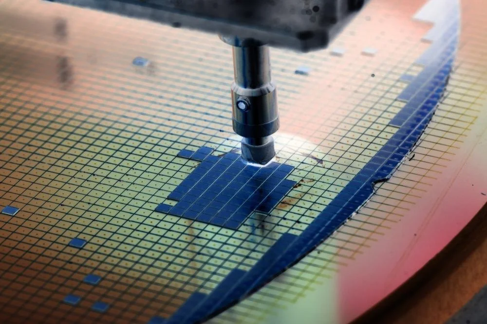
Packaging process steps
Wafer dicing:
- Diamond cutters slice wafers into individual chip units
- Each functional chip gets separated for individual packaging
Mounting and connection:
- Chips get placed on lead frames or printed circuit boards
- Small balls provide electrical connections between chip and package
- Lead frames deliver electrical signals while providing structural support
Moulding process:
- Intense heat liquefies epoxy moulding compound
- The liquid resin gets shaped into the desired external package
- This creates the final protective shell around the chip
Step 8: Testing
Final quality verification
After packaging, chips undergo comprehensive testing to ensure proper functionality. This final verification step catches any problems before products reach customers.
Testing procedures
Performance testing:
- Chips get tested under various voltage conditions
- Different electrical signal patterns verify correct operation
- Temperature testing ensures reliability across operating ranges
Data collection and analysis:
- Testing generates detailed performance data
- Engineers analyse results to identify any defects
- Feedback helps improve manufacturing and assembly processes
Final Quality Assurance: This testing phase simulates years of normal use in just hours, ensuring that chips will perform reliably throughout their expected lifespan in consumer devices.
Product identification
Once testing confirms functionality:
- The chip name gets printed on the package
- Manufacturing date and location information gets added
- Product specifications and serial numbers get included
- This traceability helps with quality control and customer support
The comprehensive testing ensures customers receive reliable products that meet their performance requirements.
Future developments in semiconductor production
Industry innovation focus
Semiconductor manufacturing continues evolving towards more sustainable and efficient production methods. Companies invest heavily in developing new techniques that reduce environmental impact while improving performance.
Innovation Focus: The semiconductor industry invests over $70 billion annually in research and development, constantly pushing the boundaries of what's physically possible in manufacturing.
Advanced manufacturing techniques
Cutting-edge technologies:
- High-K Metal Gate technology enables smaller, more efficient circuits
- Extreme Ultraviolet (EUV) lithography allows higher circuit density
- Advanced packaging techniques improve performance while reducing size
Sustainability initiatives:
- Development of more environmentally friendly manufacturing processes
- Improved energy efficiency in production facilities
- Reduced waste through better process control
These innovations help meet growing demand for more powerful, efficient semiconductor devices while addressing environmental concerns.
Key Points to Remember:
-
Silicon wafers form the foundation of all semiconductor devices, created from purified sand and processed into ultra-smooth substrates
-
Photolithography transfers circuit patterns onto wafers using photomasks and precise light exposure techniques
-
Etching processes remove unwanted material, with plasma etching preferred for its precision and higher yields
-
Thin-film deposition builds up materials at atomic levels using PVD and CVD methods to create the required electrical properties
-
Quality control occurs at multiple stages, particularly through EDS testing and final performance verification, ensuring only functional chips reach consumers
-
The entire process requires extraordinary precision - working at scales smaller than viruses to create devices containing billions of components